The computing industry has undergone a fundamental shift over the past two decades. Where once we pursued ever-faster general-purpose CPUs, we now see an explosion of specialized silicon: FPGAs in datacenters, ASICs mining cryptocurrencies, TPUs training neural networks, and custom accelerators embedded in everything from smartphones to satellites. This transition wasn’t arbitrary — it emerged from fundamental constraints in physics, economics, and the mathematics of concurrent computation.
At its philosophical core, this shift represents a profound choice between time and space — between doing many things sequentially on shared resources (concurrency through time-slicing) or doing many things simultaneously with dedicated resources (parallelism through spatial replication). General-purpose computing bet on time: one powerful CPU, rapidly context-switching between tasks, creating the illusion of simultaneity. Specialized computing bets on space: many purpose-built execution units, each doing one thing extraordinarily well, truly working in parallel.
This time-versus-space tradeoff isn’t just technical — it’s ontological. When you time-slice, you accept that “concurrent” execution is fundamentally sequential underneath, an illusion maintained through rapid switching. When you spatially distribute, you acknowledge that true parallelism requires physical resources, and that optimization means building different hardware for different problems. The former is elegant and flexible; the latter is pragmatic and performant.
The industry spent four decades pursuing the time-based model, extracting ever-more instruction-level parallelism from general-purpose CPUs. But we’ve hit fundamental limits: power walls, memory walls, and the end of Dennard scaling. Now we’re rediscovering what analog computers and ASICs always knew — sometimes you need dedicated space to solve problems efficiently.
This article traces that evolution through the lens of concurrency theory, virtualization overhead, real-world migration stories, and case studies spanning financial systems, cryptography, blockchains, and artificial intelligence. By the end, you’ll understand why the future of compute isn’t about choosing between CPUs, GPUs, FPGAs, and ASICs — it’s about orchestrating all of them.
Part 1: The Fundamental Illusion of Concurrency
Concurrency vs. Parallelism: A Crucial Distinction
Rob Pike famously said, “Concurrency is about dealing with lots of things at once. Parallelism is about doing lots of things at once.” This distinction isn’t semantic — it’s foundational to understanding why specialized hardware exists.
Concurrency is a programming model. It’s the ability to structure a program so that multiple tasks can make progress without necessarily executing simultaneously. A single-core CPU running a multithreaded application is concurrent but not parallel. The operating system rapidly switches between threads, creating the illusion that they’re all running “at once.”
Parallelism is about execution. It requires multiple physical execution resources — multiple cores, multiple machines, or dedicated hardware units — actually performing operations simultaneously. Parallelism is what happens when your four-core CPU genuinely executes four instruction streams at the same instant.
The critical insight: pure concurrency cannot exist on a single physical resource. If you have one ALU, one memory bus, one execution pipeline, you can only do one thing at a time. Everything else is scheduling theater.
The Time-Slicing Illusion
Modern operating systems are masterful illusionists. When you see twenty processes “running” on your laptop’s eight-core CPU, you’re witnessing an elaborate performance of context switching, time slicing, and preemptive scheduling.
The kernel maintains a ready queue of runnable threads. Every few milliseconds (typically 1–10ms depending on the scheduler), it saves the current thread’s state — registers, program counter, stack pointer — and loads another thread’s state. This context switch has overhead: flushing TLB entries, polluting CPU caches, and burning cycles on bookkeeping. On x86, a context switch typically costs 1–2 microseconds of pure overhead, plus additional cycles for cache warmup.
For most applications, this overhead is acceptable. But for high-frequency trading systems processing market data, or for real-time control systems managing industrial equipment, these microsecond delays are catastrophic. This is where the first cracks appear in the general-purpose computing model.
Cloud Virtualization: Concurrency Squared
Cloud computing adds another layer of illusion. When AWS advertises a c5.2xlarge instance with "8 vCPUs," they're not giving you eight dedicated physical cores. You're receiving eight virtual CPUs—time-sliced shares of physical CPU cores that may be simultaneously allocated to dozens of other tenants.
The hypervisor (KVM, Xen, or VMware ESXi) performs a scheduling dance at two levels:
Guest OS scheduling: Inside your VM, Linux or Windows schedules threads across vCPUs Hypervisor scheduling: The hypervisor schedules vCPUs across physical cores (pCPUs) This creates what I call “concurrency squared” — scheduling on top of scheduling. Each layer adds latency, jitter, and unpredictability.
CPU Overcommit: The Dirty Secret
In production clouds, CPU overcommit ratios typically range from 3:1 to 10:1. A 32-core physical server might support 200+ vCPUs across all VMs. This works because most workloads are idle most of the time. But when multiple VMs suddenly demand CPU — perhaps during synchronized cron jobs or coordinated load spikes — the hypervisor’s scheduler becomes a bottleneck.
You’ve requested CPU time. Your vCPU is ready to run. But the hypervisor has scheduled four other vCPUs on that pCPU, and they’re executing their time slices. You wait. This wait isn’t reflected in your VM’s CPU utilization metrics — from inside the VM, you simply experience mysterious latency spikes that don’t correlate with your application’s behavior.
The vCPU Scheduling Tax
Modern hypervisors use sophisticated algorithms — Completely Fair Scheduler (CFS) in KVM, Credit Scheduler in Xen — to distribute CPU time fairly. But “fair” doesn’t mean “predictable” or “low-latency.”
Consider a latency-sensitive database query that should complete in 500 microseconds. On bare metal, it reliably does. In a virtualized environment with moderate overcommit:
Context switch overhead adds 1–2μs per vCPU switch Hypervisor scheduling latency adds 10–100μs of jitter Memory access patterns change due to NUMA effects Cache behavior degrades from competing tenants Your 500μs query now occasionally takes 1–2ms, with unpredictable tail latencies. The P99 latency explodes because sometimes your vCPU simply isn’t scheduled when you need it.
This isn’t a bug — it’s the fundamental cost of multiplexing. And it’s why high-performance systems increasingly demand dedicated hardware.
Part 2: Real-World Performance Impact of Virtualization
The Noisy Neighbor Problem
In 2013, researchers at Duke University published a landmark study showing that virtualization overhead could vary by 400% depending on co-located workloads. They ran identical benchmarks on identical VM configurations and observed wildly different performance based solely on what other tenants were doing.
The culprits:
LLC (Last Level Cache) contention: Modern CPUs share L3 cache across cores. When neighbors have large working sets, your cache hit rate plummets Memory bandwidth saturation: DRAM bandwidth is shared. A neighbor running memory-intensive workloads starves your application TLB shootdowns: When one core modifies page tables, it must invalidate TLB entries on other cores via inter-processor interrupts Power management: Modern CPUs throttle frequency when thermal limits are reached. Your neighbor’s CPU-intensive task triggers throttling that affects your core AWS’s response to this was introducing “dedicated instances” and eventually “bare metal” instances like i3.metal, where you receive the entire physical server. The premium for these instances reflects the true cost of eliminating multiplexing overhead.
Case Study: Latency-Sensitive Trading Systems High-frequency trading firms learned this lesson painfully in the early 2010s. Initial attempts to run market data feed handlers in EC2 or Azure failed spectacularly — not because the average throughput was insufficient, but because tail latencies were unpredictable.
A typical NASDAQ TotalView feed delivers 10–15 million messages per second during market hours. Processing each message in under 10 microseconds is table stakes. But in virtualized environments, occasional 100–500μs pauses — caused by hypervisor scheduling, vCPU migration, or noisy neighbors — meant missing critical price updates.
The industry’s response was threefold:
Colocation: Move compute into exchange datacenters, minimizing network latency Bare metal: Eliminate hypervisors entirely Specialized hardware: Offload critical paths to FPGAs This third response is where our story of specialized silicon truly begins.
Part 3: Migration Stories — From CPUs to Specialized Silicon
NASDAQ Feed Handlers: The FPGA Revolution
In 2009, NASDAQ partnered with multiple vendors to develop FPGA-based feed handlers. These devices sit directly on the network, parse market data protocols (ITCH, OUCH), and deliver structured messages to trading algorithms — all in hardware, with sub-microsecond latency.
Why FPGAs instead of faster CPUs?
Determinism: An FPGA’s behavior is defined by its circuit configuration. There’s no instruction fetching, no branch prediction, no cache misses. Every packet follows the same path through fixed logic gates. Processing latency has single-digit nanosecond jitter.
Pipelining: FPGAs excel at streaming data through deeply pipelined architectures. While stage 1 processes packet N, stage 2 processes N-1, stage 3 processes N-2, and so on. You achieve one-packet-per-cycle throughput even when each packet requires dozens of operations.
Parallelism: Need to parse 10 different market data feeds simultaneously? Instantiate 10 parallel parser circuits. An FPGA doesn’t schedule — it literally builds separate hardware for each task.
The result: NASDAQ feed handlers that process messages in 300–500 nanoseconds, compared to 5–10 microseconds for optimized CPU implementations. That 20x latency reduction translates directly into trading advantage.
Microsoft Project Catapult: Bing on FPGAs
In 2014, Microsoft announced Project Catapult, an ambitious effort to accelerate Bing search using FPGAs. The initial deployment placed FPGAs on the network path, offloading ranking algorithms directly in hardware.
The challenge Bing faced was computational: ranking search results requires scoring millions of potential results against hundreds of features using machine learning models. On CPUs, this consumed significant datacenter capacity and added latency to search results.
Microsoft’s FPGA solution:
Each server received a Stratix V FPGA connected via PCIe Ranking models compiled to FPGA circuits using Altera’s OpenCL toolchain FPGAs processed ranking in parallel with CPU query parsing Results were dramatic: 2x throughput improvement and 50% latency reduction for ranking workloads, with better energy efficiency. But perhaps more importantly, Microsoft gained reconfigurability — they could update ranking algorithms by reprogramming FPGAs, without hardware replacement.
This deployment taught the industry several lessons:
FPGAs work best for datapath operations, not control logic Integration complexity is real — PCIe bottlenecks, coherency issues, and programming difficulty matter TCO isn’t just about performance — power efficiency and flexibility factor heavily By 2020, Microsoft had deployed FPGAs across hundreds of thousands of servers, extending their use from Bing to Azure networking (SmartNICs) and AI inference.
Bitcoin Mining: The Complete ASIC Journey
Bitcoin mining provides perhaps the clearest narrative of specialization. The evolution happened rapidly, driven by pure economics:
Press enter or click to view image in full size
Timeline infographic showing Bitcoin mining evolution from 2009–2023: CPU (10–20 MH/s) → GPU (200–400 MH/s) → FPGA (800–1000 MH/s) → ASIC (140 TH/s), with relative power efficiency improvements 2009–2010: CPU Mining Early Bitcoin miners used general-purpose CPUs. Satoshi Nakamoto’s original client included CPU mining code. A high-end Intel CPU might achieve 10–20 million hashes per second (MH/s). This phase lasted about a year.
2010–2011: GPU Mining Miners discovered that GPUs, with thousands of ALUs designed for parallel graphics rendering, excelled at SHA-256 hashing. A mid-range GPU could achieve 200–400 MH/s — 20x better than CPUs. Overnight, CPU mining became uneconomical.
The reason GPUs worked better is fundamental: SHA-256 is embarrassingly parallel. Each hash attempt is independent. GPUs don’t need sophisticated branch prediction, out-of-order execution, or large caches — they need thousands of simple ALUs churning through hashes.
2011–2013: FPGA Mining Dedicated miners invested in FPGAs, which offered 2–3x better performance-per-watt than GPUs and lower latency. FPGAs could instantiate dozens of optimized SHA-256 pipeline circuits, achieving 800–1000 MH/s while consuming less power than GPU rigs.
But FPGAs were expensive (thousands of dollars), difficult to program, and had limited production scale. They were an intermediate step.
2013-Present: ASIC Dominance The first Bitcoin ASICs appeared in 2013. These chips did one thing: SHA-256 double-hashing for Bitcoin’s proof-of-work. They couldn’t run Windows, render graphics, or solve other problems — but they absolutely dominated Bitcoin mining.
Modern Bitcoin ASICs like Bitmain’s Antminer S19 XP achieve 140 TH/s (terahashes per second) — 140 trillion hashes per second. That’s 7 million times faster than early CPU miners. They achieve this through:
Circuit optimization: Every transistor dedicated to SHA-256 Massive parallelism: Thousands of SHA-256 cores on a single chip Process technology: 5nm or 7nm fabrication (vs. 45nm for early ASICs) Power efficiency: ~20 joules per terahash (vs. thousands for GPUs) Today, the Bitcoin network’s total hashrate exceeds 500 EH/s (exahashes). This level of computational power isn’t just beyond CPU or GPU mining — it represents more specialized hashing computation than all other computing in human history combined.
The economic driver is simple: electricity costs dominate mining. An ASIC that’s 100x more power-efficient than a GPU will 100x more profit per dollar of electricity. In competitive mining, efficiency isn’t an advantage — it’s survival.
Networking ASICs: Broadcom’s Silicon Monopoly While Bitcoin ASICs make headlines, networking ASICs quietly revolutionized datacenters. Companies like Broadcom dominate the market for Ethernet switch chips — the ASICs that power datacenter networks.
Broadcom’s Trident and Tomahawk families are purpose-built for packet forwarding:
Packet parsing: Hardware state machines parse Ethernet, IP, TCP headers at line rate Lookup engines: Dedicated TCAM (Ternary Content Addressable Memory) performs routing table lookups in nanoseconds Queueing: Sophisticated hardware schedulers manage packet buffers, QoS, and congestion control Multicast replication: Hardware duplicates packets for multicast/broadcast A Tomahawk 4 ASIC can forward 25.6 Tbps (terabits per second) of traffic — that’s 320 million packets per second at maximum packet size, or billions of packets per second for minimum-sized packets. No CPU could approach this throughput.
Why ASICs instead of programmable solutions?
Latency: Sub-microsecond port-to-port latency is critical for datacenter networks Power: Forwarding packets with CPUs would require megawatts of power Scale: Google, AWS, and Meta each deploy millions of switch ports Cost: A $500 ASIC replaces what would require dozens of CPU cores The tradeoff is flexibility. Programming these ASICs requires specialized languages like P4, and they can’t implement arbitrary protocols. But for the 99% case of Ethernet/IP forwarding, they’re unbeatable.
Interestingly, this created opportunities for SmartNICs — network cards with integrated FPGAs or DPUs (Data Processing Units) that bridge the gap between ASIC rigidity and CPU flexibility.
Part 4: Hardware Security Modules — Cryptographic ASICs in Practice
What HSMs Actually Are
Hardware Security Modules occupy a unique position in the specialized silicon landscape. Unlike ASICs designed for performance, HSMs prioritize security and tamper resistance. But at their core, they rely heavily on cryptographic ASICs to achieve their security properties.
An HSM is fundamentally a secure computing environment — a small, hardened computer designed to protect cryptographic keys and perform cryptographic operations without ever exposing key material. Think of it as a safe that can perform calculations on secrets without opening.
HSM Internal Architecture
Modern HSMs like Thales Luna, AWS CloudHSM, or YubiHSM contain several specialized components:
Secure Microcontroller: Often an ARM-based processor running hardened firmware. This handles cryptographic operations, key management, and access control. But critically, it’s not a general-purpose CPU — it’s a reduced instruction set processor optimized for security.
Cryptographic Accelerators (ASICs): Dedicated silicon for AES, RSA, ECC, and SHA operations. These ASICs implement constant-time algorithms immune to timing side-channels. A software implementation of RSA on a general CPU might leak key bits through timing variations; an ASIC implementation executes in precisely the same time regardless of input.
True Random Number Generator (TRNG): Hardware entropy source, typically based on physical phenomena like thermal noise or quantum effects. Secure cryptography requires high-quality randomness — you can’t fake entropy in software.
Tamper Detection Mesh: Physical circuitry that detects drilling, probing, voltage glitching, and other physical attacks. If triggered, the HSM immediately zeros memory and destroys keys.
Secure Memory: Battery-backed RAM or non-volatile memory with encryption and authentication. Key material never exists in plaintext outside the secure boundary.
Cryptographic Boundary: FIPS 140–2/140–3 certification defines physical and logical boundaries. Everything outside is untrusted; everything inside is protected.
Why HSMs Depend on ASICs
The cryptographic ASICs inside HSMs serve three critical purposes:
Performance: RSA-4096 key generation or ECC signing might take 100ms in software on an embedded processor. A cryptographic ASIC performs the same operation in 1–10ms. When you’re signing thousands of TLS certificates per second, this matters.
Constant-Time Execution: Software cryptography is vulnerable to timing attacks — attackers measure execution time to infer bits of the secret key. ASICs implement operations in fixed-time hardware pipelines, eliminating timing channels.
Side-Channel Resistance: Beyond timing, ASICs resist power analysis (measuring power consumption to infer operations) and electromagnetic analysis (detecting EM emissions). They achieve this through balanced logic gates, noise generators, and careful layout.
Without these ASICs, an HSM would be too slow for production use and vulnerable to sophisticated attacks. The HSM’s security properties emerge from the combination of tamper-resistant packaging, secure microcontroller, and cryptographic ASICs working together.
HashiCorp Vault and HSMs: A Common Misconception
This is where confusion often arises. HashiCorp Vault is frequently misunderstood as an HSM replacement. It’s not.
Vault is a secrets management system — a sophisticated API layer, access control framework, and encryption-as-a-service platform. It stores secrets, generates dynamic credentials, rotates keys, and provides audit logs. But Vault itself runs on general-purpose servers as a software application.
Vault + HSM Integration: Vault can integrate with HSMs in two ways:
Seal/Unseal with HSM: The master key that encrypts Vault’s storage backend can be protected by an HSM. Instead of requiring operators to manually enter unseal keys on startup, Vault authenticates to the HSM and retrieves the master key. This is “auto-unseal.” PKCS#11 Cryptographic Operations: Vault’s Transit secrets engine can offload cryptographic operations to an HSM via PKCS#11. When you request Vault to sign data, Vault forwards the request to the HSM, which performs signing using a key that never leaves the HSM’s boundary. Why Vault Isn’t an HSM:
Vault runs on general-purpose servers without physical tamper resistance Vault’s key material can be extracted if you compromise the operating system or hypervisor Vault doesn’t have dedicated cryptographic ASICs — it uses CPU-based crypto libraries Vault doesn’t meet FIPS 140–2 Level 3/4 requirements for physical security The value proposition is different. Vault provides developer ergonomics, cloud integration, dynamic secrets, and policy-based access control. HSMs provide FIPS-certified physical security and cryptographic assurance. Most organizations use both: Vault as the API layer and management plane, HSM as the root of trust.
For truly sensitive operations — signing root CA certificates, protecting payment card PINs, securing blockchain validators — you need real HSMs. For broader secrets management across cloud infrastructure, Vault is the right tool.
Part 5: ASICs in Blockchain Consensus
The relationship between blockchains and ASICs varies dramatically based on consensus mechanism. Understanding this reveals deeper truths about why specialized silicon emerges.
Bitcoin: ASIC-Dominated by Design
Bitcoin’s proof-of-work (PoW) consensus requires miners to find a nonce such that the block’s SHA-256 hash is below a target threshold. This is pure brute force — try billions of nonces until one works.
SHA-256 is a deterministic, parallelizable, compute-intensive function with no memory dependency — the perfect ASIC target. Once Bitcoin ASICs became available, CPU and GPU mining died instantly. Today, mining Bitcoin without ASICs is like fighting a tank with a stick.
This has consequences:
Centralization: ASIC manufacturing requires multi-billion dollar fabs, typically TSMC or Samsung. Only a few companies (Bitmain, MicroBT, Canaan) dominate production. This concentrates power.
Barrier to Entry: Participating in Bitcoin mining now requires capital investments of tens or hundreds of thousands of dollars for competitive hardware, plus cheap electricity and cooling infrastructure.
Security: Ironically, ASIC dominance increases Bitcoin’s security. To execute a 51% attack, you’d need to manufacture more ASICs than all existing miners combined — economically impractical.
Ethereum Classic and ASIC-Resistance
Ethereum originally used Ethash, a memory-hard PoW algorithm designed to resist ASICs. The idea: require algorithms that depend heavily on memory bandwidth (not just computation), making ASICs less advantageous compared to commodity GPUs with high-bandwidth GDDR memory.
Memory-hardness works by forcing the algorithm to randomly access a large dataset (the DAG, or Directed Acyclic Graph) during hashing. CPUs and ASICs have limited memory bandwidth; GPUs have very high bandwidth due to their design for texture operations.
Did it work? Partially. For several years, Ethereum mining remained GPU-dominated. But eventually, Bitmain released Ethash ASICs (Antminer E3, E9) that achieved 2–3x better efficiency than GPUs. Memory prices dropped, ASIC designers integrated high-bandwidth memory, and economics won.
The lesson: you can resist ASICs temporarily, but if the economic incentive is large enough, engineers will build them.
Ethereum and Cardano: Proof-of-Stake Changes Everything
In September 2022, Ethereum transitioned from proof-of-work to proof-of-stake (PoS). This fundamentally eliminated the role of ASICs in consensus.
PoS doesn’t require mining — instead, validators stake capital (ETH) and are selected to propose blocks based on their stake. Block validation involves:
Verifying cryptographic signatures (ECDSA or BLS) Executing smart contract transactions (EVM bytecode) Updating state trees (Merkle Patricia tries) None of these operations benefit significantly from ASICs:
Signature Verification: While you could build an ASIC for ECDSA or BLS signatures, the throughput demands are modest. Validators process blocks every 12 seconds, not millions of hashes per second. A standard CPU handles this trivially.
Smart Contract Execution: The EVM is a general-purpose virtual machine. Compiling arbitrary smart contracts to ASICs is impossible — you’d need to know all possible programs in advance.
State Management: Block validation is I/O bound (reading/writing state to disk) rather than compute-bound. Faster CPUs don’t help much; faster SSDs do.
Cardano, which launched with proof-of-stake (Ouroboros consensus), never had an ASIC mining phase. The consensus mechanism simply doesn’t include a parallelizable, compute-intensive problem suitable for ASICs.
The broader implication: PoS blockchains effectively use “capital investment” (staking) as their security mechanism, rather than “computational expenditure” (mining). This shift eliminates the specialized hardware arms race entirely.
ZK-Proof Accelerators: The Next Frontier
While PoS blockchains don’t need mining ASICs, a new class of specialized hardware is emerging: zero-knowledge proof accelerators.
Zero-knowledge proofs (ZK-proofs) allow proving computational statements without revealing inputs. Modern blockchains use ZK-proofs for:
ZK-Rollups: Scaling layer-2 solutions that batch thousands of transactions and prove their validity with a single proof Privacy: Zcash and other privacy coins use ZK-SNARKs to hide transaction details Interoperability: Proving execution on one chain to another The problem: generating ZK-proofs is extremely compute-intensive. Proving a simple transaction might require billions of cryptographic operations — elliptic curve pairings, polynomial commitments, hash functions.
Companies like Supranational, Ingonyama, and Ulvetanna are building ZK-proof accelerators — FPGAs and ASICs optimized for elliptic curve operations, particularly the MSM (multi-scalar multiplication) primitive that dominates ZK-proof generation time.
Early results show 100–1000x speedups compared to CPU implementations. This isn’t just performance improvement — it’s enabling new applications. Without accelerators, generating proofs for complex ZK-rollup blocks might take hours. With accelerators, it takes seconds, making real-time blockchain scaling viable.
This represents a fascinating evolution: blockchains moving from ASIC-based consensus (Bitcoin) to no-ASIC consensus (Ethereum PoS) to ASIC-accelerated cryptography (ZK-proofs). The specialized hardware adapts to wherever the computational bottleneck appears.
Part 6: ASICs in Modern AI
The AI hardware landscape has become one of the most dynamic areas of specialized silicon development. While GPUs dominate training, ASICs are rapidly capturing inference workloads — and the reasons reveal fundamental truths about when specialization makes sense.
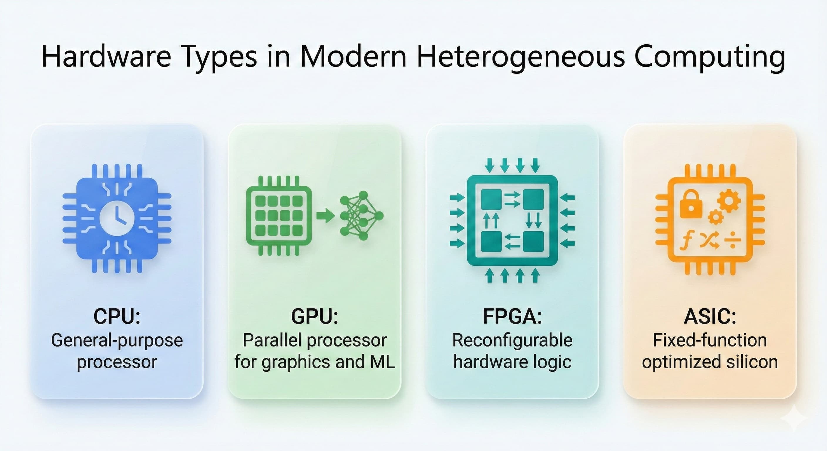
The GPU, FPGA, ASIC Tradeoffs
GPUs (Graphics Processing Units) were originally designed for rendering graphics, but their architecture — thousands of simple cores, high memory bandwidth, flexible programming model — made them accidentally perfect for deep learning. NVIDIA’s CUDA ecosystem provided the software stack that cemented GPU dominance.
GPU strengths:
High flexibility: run any neural network architecture Mature tooling: PyTorch and TensorFlow have excellent GPU support Fast development cycles: train new architectures without hardware changes Strong numerical precision control GPU weaknesses:
Power inefficiency: general-purpose features waste energy High cost: A100/H100 GPUs cost $10,000-$40,000 each Limited batch size: memory constraints limit throughput PCIe bottleneck: moving data to/from GPUs adds latency FPGAs offer a middle ground. They’re reconfigurable — you can implement custom neural network architectures in hardware, then reprogram them when architectures evolve.
FPGA strengths:
Lower power than GPUs for inference Customizable precision: use 8-bit, 4-bit, or even 2-bit arithmetic Deterministic latency: no OS scheduling overhead Reconfigurable: update as models change FPGA weaknesses:
Programming complexity: requires HDL expertise or specialized tools Lower peak performance than GPUs or ASICs Higher cost than ASICs at scale Limited floating-point performance ASICs are fixed-function chips designed for specific workloads. Once manufactured, they can’t be changed — but within their domain, they’re unbeatable on performance, power, and cost at volume.
ASIC strengths:
Maximum performance per watt Lowest cost at high volume Optimized data paths: no wasted transistors Predictable behavior: no software stack variability ASIC weaknesses:
No flexibility: if your workload changes, you need new chips High NRE (non-recurring engineering) costs: $10M-$100M to design and tape out Long development cycles: 18–24 months from design to production Risk: if you guessed wrong about workload requirements, you’ve built expensive paperweights
Google TPU: The Pioneer
In 2016, Google unveiled the Tensor Processing Unit (TPU), the first major AI ASIC. The TPU addressed a specific problem: inference for neural networks in Google’s datacenters (search ranking, translation, image recognition).
The TPU’s architecture reflects its constraints:
Systolic Array: A 256×256 grid of multiply-accumulate (MAC) units. Data flows through this array in a wave pattern, with each cell performing one MAC operation per cycle. This achieves 92 TOPS (tera-operations per second) for 8-bit integer operations.
Reduced Precision: TPUs use 8-bit integers for inference (vs. 32-bit floating point in training). Neural networks are surprisingly robust to quantization — you lose minimal accuracy but gain 4x throughput and power savings.
Large On-Chip Memory: 28 MB of on-chip memory (vs. 6 MB in contemporary CPUs) reduces DRAM accesses. Memory access is often the bottleneck in inference, not computation.
Deterministic Execution: No caches, no branch prediction, no speculative execution. Every operation takes a fixed number of cycles. This makes latency predictable — critical for user-facing services.
The results were striking: 30–80x better performance-per-watt than GPUs or CPUs for inference. Google deployed TPUs across their datacenters, handling billions of inference requests daily.
But TPUs have limitations:
Only support TensorFlow (initially) Fixed architecture: can’t adapt to radically new model designs Not suitable for training (early versions) Require large batch sizes for efficiency AWS Trainium and Inferentia: Custom Cloud Silicon AWS recognized that most machine learning workloads follow predictable patterns. While researchers constantly invent new architectures, production inference workloads typically run mature models at massive scale. This creates an opening for ASICs.
Inferentia (2019) targets inference:
Optimized for transformer models (BERT, GPT) Supports INT8, FP16, and BF16 precision Four NeuronCores per chip, each with tensor engines and vector engines Integrated into EC2 instances (Inf1, Inf2) Trainium (2021) targets training:
Supports FP32, FP16, BF16, and even stochastic rounding for training 32GB HBM2e memory per chip Custom interconnect (NeuronLink) for multi-chip scaling Priced 50% lower than comparable GPU instances AWS’s strategy is different from Google’s. While Google designs TPUs exclusively for internal use, AWS must support diverse customer workloads. This constrains how specialized they can be — hence support for multiple precisions, general matrix multiply operations, and compatibility with PyTorch and TensorFlow.
The economic argument for Trainium/Inferentia is compelling: if you’re running stable inference workloads at scale (recommendation engines, fraud detection, content moderation), why pay for GPU flexibility you don’t need? A 50% cost reduction translates to millions of dollars annually for large ML deployments.
Cerebras: The Wafer-Scale Engine
Cerebras took a radical approach: instead of building chips that fit on small silicon dies, they built a single chip that spans an entire 300mm silicon wafer. The Cerebras WSE-2 (Wafer-Scale Engine 2) contains:
850,000 cores 40 GB of on-chip SRAM 20 PB/s memory bandwidth (purely on-chip) 220 trillion transistors The insight: neural network training is bottlenecked by memory bandwidth, not computation. GPUs spend most of their time waiting for data from DRAM. Cerebras eliminates this by putting all weights and activations in on-chip SRAM, achieving thousands of times higher bandwidth.
This enables training models that don’t fit on GPU clusters. Large language models with hundreds of billions of parameters can train on a single Cerebras machine, avoiding the complexity of distributed training across hundreds of GPUs.
The tradeoff: you need workloads that benefit from massive parallelism and fit Cerebras’s architecture. Not all models do. And at $2–3 million per system, this is capital-intensive.
But for specific workloads — training large transformers, running massive simulations — Cerebras demonstrates that specialized architectures can unlock entirely new scales of computation.
Tesla FSD: ASICs in Production Vehicles
Tesla’s Full Self-Driving (FSD) computer represents ASICs moving from datacenters to edge devices. Every Tesla vehicle since 2019 includes custom neural network accelerators designed by Tesla’s chip team.
The FSD chip contains:
Two independent neural network accelerators (for redundancy) 36 TOPS per accelerator at FP32-equivalent accuracy 32 MB SRAM per accelerator Integrated ISP (image signal processor) for camera inputs Why custom silicon instead of off-the-shelf GPUs?
Power: A car’s electrical system provides limited power. The FSD chip achieves 2x better performance per watt than contemporary GPUs, critical for battery-powered vehicles.
Latency: Autonomous driving requires sub-100ms reaction times. Deterministic, low-latency inference is easier with dedicated hardware than with a GPU running Linux and a deep learning framework.
Cost: At $1000–2000 per chip in volume production, custom ASICs are cheaper than equivalent GPU solutions.
Integration: The chip integrates camera ISPs, neural network accelerators, and safety subsystems on a single die, minimizing system complexity.
Tesla’s vertical integration — designing chips, training models, collecting data from millions of vehicles — creates advantages that traditional automotive suppliers struggle to match. The ASIC is optimized for Tesla’s specific neural network architectures (HydraNet for vision), which evolved together with the hardware.
Why ASICs Won’t Completely Replace GPUs
Despite these success stories, ASICs won’t eliminate GPUs from AI workflows. The reason comes back to our time-versus-space tradeoff and the nature of research versus production.
Research velocity demands flexibility. Neural network architectures evolve constantly — transformers, diffusion models, mixture-of-experts, state-space models. Each requires different computational patterns. An ASIC designed for 2020-era ResNets is useless for 2023-era transformers. GPUs, being programmable, adapt to new architectures through software updates.
Training requires numerical precision and experimentation. While inference tolerates INT8 quantization, training typically needs FP32 or at minimum BF16. ASICs sacrifice precision for efficiency; GPUs maintain flexibility. And during research, you’re constantly tweaking hyperparameters, adjusting architectures, and debugging — all easier with general-purpose hardware.
Economic viability requires scale and stability. An ASIC costs $10–100M to design and tape out. You need to manufacture millions of units to amortize that cost. This only makes sense for stable, high-volume workloads — inference for mature models, not exploratory research.
The result: a natural division of labor. GPUs dominate training and research. ASICs dominate production inference for mature models. FPGAs occupy the middle ground — reconfigurable accelerators for workloads that are stable enough to warrant custom hardware but still evolving.
This mirrors what happened in networking: ASICs handle standard packet forwarding, but SmartNICs with FPGAs or DPUs handle programmable packet processing. Each technology finds its niche based on the stability-flexibility tradeoff.
Part 7: The Heterogeneous Future
We’ve journeyed from concurrency theory through virtualization overhead, examined migrations to specialized silicon across finance, cryptography, blockchains, and AI, and explored the architectural tradeoffs driving these transitions. Now we must synthesize: what does the future actually look like?
The End of Homogeneous Computing
The era of “just make CPUs faster” ended with the death of Dennard scaling around 2005. Since then, we’ve pursued three strategies simultaneously:
Horizontal scaling: More servers, distributed systems Vertical heterogeneity: Different processors on the same die (big.LITTLE, ARM + NPU + ISP) Domain-specific acceleration: Purpose-built silicon for specific workloads The future isn’t choosing one strategy — it’s orchestrating all three intelligently.
The Layered Architecture of Modern Systems Think of compute as a stack, where each layer has different optimization criteria:
Layer 1 — Control Plane (CPUs): Orchestration, scheduling, business logic, exception handling. Workloads are unpredictable, require branching and complex control flow, and benefit from general-purpose flexibility. CPUs remain optimal here.
Layer 2 — Data Plane (GPUs/FPGAs): Data processing, analytics, ML training. Workloads involve regular, data-parallel operations but still evolve frequently. GPUs provide the right balance of performance and flexibility. FPGAs fit when latency determinism matters.
Layer 3 — Critical Path (ASICs): High-volume, latency-sensitive, stable operations. Network packet forwarding, production ML inference, cryptographic operations, blockchain consensus. ASICs dominate through pure efficiency — when you’ve settled on what needs to be fast, build hardware specifically for it.
Modern applications span all three layers. Consider a cloud-based recommendation system:
CPUs handle user requests, database queries, API orchestration GPUs train recommendation models on historical data ASICs (Inferentia) serve real-time predictions to millions of users FPGAs (SmartNICs) accelerate network encryption and load balancing No single technology could handle all these efficiently. The heterogeneous approach optimizes each layer independently while maintaining composability.
Economic and Environmental Drivers
The shift to specialized silicon isn’t purely technical — it’s economically and environmentally necessary.
Power efficiency: Datacenters now consume 1–2% of global electricity. As AI and cloud computing grow, this becomes unsustainable. ASICs deliver 10–100x better performance per watt than CPUs for targeted workloads. At hyperscale, this translates to billions of dollars in electricity costs and meaningful carbon emission reductions.
Total Cost of Ownership: Yes, designing an ASIC costs tens of millions. But if you’re deploying 100,000 inference servers, spending $50M on custom silicon to reduce per-server costs by $1000 saves $50M in the first deployment alone — and continues saving with each subsequent generation.
Latency is money: In high-frequency trading, every microsecond advantage translates to millions in annual profit. In web services, every 100ms of latency reduces conversion rates by 1%. When latency directly impacts revenue, spending on specialized hardware becomes an obvious investment.
Competitive moats: Companies with custom silicon gain architectural advantages competitors can’t easily replicate. Google’s TPUs, Tesla’s FSD chips, Apple’s Neural Engine — these create differentiation in increasingly commoditized markets.
The Software Abstraction Challenge
Heterogeneous computing creates a profound software challenge: how do developers target this diverse hardware landscape without going insane?
The industry is converging on several approaches:
High-level frameworks with compiler backends: PyTorch and TensorFlow abstract away hardware details. You write model code once; the framework compiles to CPUs, GPUs, TPUs, or other accelerators. This works well for data-parallel workloads like ML.
Domain-specific languages: P4 for networking, OpenCL for FPGAs, Triton for GPU kernels. These languages capture domain invariants while remaining hardware-agnostic enough to target multiple backends.
Heterogeneous runtime systems: CUDA, ROCm, oneAPI, OpenCL provide runtime abstractions for dispatching work to accelerators. Applications remain largely unaware of hardware details.
Composable primitives: Libraries like cuBLAS, cuDNN, MKL provide heavily optimized implementations of common operations. Applications compose these primitives rather than writing low-level code.
The key insight: abstraction layers must align with hardware capabilities. You can’t abstract away the fundamental differences between sequential CPUs and massively parallel ASICs — but you can build interfaces that let developers express parallelism naturally and let compilers target appropriate hardware.
When to Choose Each Technology
For architects designing new systems, here’s a decision framework:
Choose CPUs when:
Control flow is unpredictable and complex Workload characteristics change frequently Development velocity matters more than peak performance Scale is modest (not worth specialization overhead) Choose GPUs when:
Workload is data-parallel but still evolving You need floating-point precision Fast iteration on algorithms is critical Mature software ecosystems exist (ML, graphics, HPC) Choose FPGAs when:
Latency determinism is critical Workload is stable but may evolve over years You need custom bit-width arithmetic Volume doesn’t justify ASIC development Integration with existing systems via standard interfaces Choose ASICs when:
Workload is completely stable and high-volume Maximum efficiency is critical (power, cost, or performance) You have the scale to amortize NRE costs Competitive advantage justifies the investment Design iteration is acceptable (18–24 month cycles) Most large-scale systems end up using combinations of all four, each optimized for different components of the overall workload.
The Cambrian Explosion of Accelerators
We’re witnessing an explosion of specialized accelerators across every domain:
Networking: DPUs (Bluefield, IPU), SmartNICs, programmable switches Storage: Computational storage (Samsung SmartSSD), NVMe acceleration Security: Cryptographic accelerators, secure enclaves (SGX, SEV) Video: H.264/H.265/AV1 encoders, AI upscalers Audio: Neural codec acceleration, spatial audio processing Compression: Zstandard accelerators, gzip offload engines Each represents the same pattern: identifying a compute-intensive, stable workload and moving it from software on CPUs to dedicated hardware.
This Cambrian explosion will continue until we hit economic limits — until the cost of designing and integrating specialized hardware exceeds the savings from improved efficiency. We’re nowhere near that limit yet.
Challenges and Risks
Heterogeneous computing isn’t without serious challenges:
Complexity: Modern system designs now require understanding CPUs, GPUs, FPGAs, ASICs, interconnects, memory hierarchies, and their interactions. The expertise barrier is high.
Integration overhead: Moving data between different compute domains incurs latency and power costs. PCIe transfers, memory copies, and synchronization add up. Sometimes the integration overhead exceeds the acceleration benefit.
Vendor lock-in: Specialized hardware often ties you to specific vendors or ecosystems. CUDA locks you into NVIDIA; TPUs lock you into Google Cloud. Portability becomes difficult.
Development velocity: Updating an ASIC requires a new tape-out — 18+ months and millions of dollars. If your workload requirements change faster than that, specialization backfires.
Testing and validation: Heterogeneous systems are harder to test, debug, and validate. The interaction between components creates emergent behaviors difficult to predict or reproduce.
Skills gap: Most engineers learned on homogeneous CPU architectures. Designing, programming, and optimizing heterogeneous systems requires new skills the industry is still developing.
These challenges explain why specialized silicon adoption happens gradually, starting with the largest-scale, highest-value workloads and expanding as tools mature.
Conclusion: Embracing Heterogeneity
The evolution from general-purpose CPUs to specialized silicon isn’t a temporary trend — it’s a fundamental response to the end of Moore’s Law dividends. When you can no longer make general-purpose processors much faster, you build specialized processors that are dramatically faster for specific tasks.
This returns us to our opening philosophical question: time versus space, concurrency versus parallelism, flexibility versus efficiency. For decades, we optimized for flexibility — one CPU to rule them all, rapidly context-switching between diverse workloads. That approach hit physical limits.
Now we’re optimizing for efficiency by embracing spatial parallelism — many specialized compute units, each excellent at specific tasks, working simultaneously. This sacrifices some flexibility but delivers orders-of-magnitude improvements in performance, power efficiency, and cost at scale.
The future of computing is unambiguously heterogeneous. Your datacenter will contain CPUs for orchestration, GPUs for flexible data-parallel workloads, FPGAs for reconfigurable acceleration, and ASICs for high-volume specialized tasks. Your smartphone already contains this heterogeneity: ARM CPU cores, GPU, Neural Engine, ISP, video codec accelerators, and secure enclave processors.
Success in this world requires new skills:
Understanding which workloads benefit from specialization Architecting systems to cleanly separate control plane from data plane Designing interfaces that abstract hardware details appropriately Balancing performance, flexibility, cost, and integration complexity The engineers and organizations that master heterogeneous computing will build the next generation of impossibly fast, efficient, and capable systems. Those that cling to homogeneous, general-purpose architectures will find themselves unable to compete on performance, cost, or power efficiency.
The age of specialized silicon has arrived. The question isn’t whether to adopt it — it’s how quickly you can learn to orchestrate it effectively.
Thanks to the teams at Google (TPU), AWS (Trainium/Inferentia), Tesla (FSD), and the broader hardware acceleration community for their pioneering work making specialized silicon accessible. Special thanks to the FPGA and ASIC design engineers whose work remains largely invisible but enables the modern computing landscape.